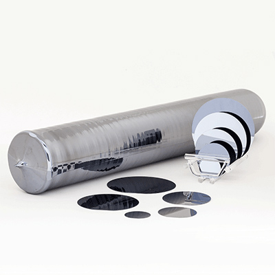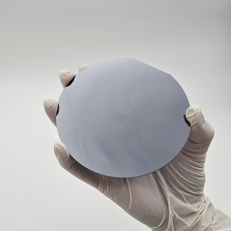
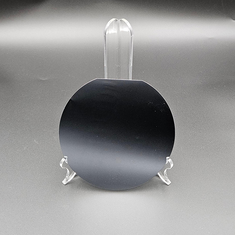
Ultra Flat Silicon Wafers
Silicon Wafer

-
+86-17701852595 WhatsApp
-
sales@plutosemitech.com Email
Ultra Flat Wafers refer to high-precision semiconductor substrate materials that achieve extremely low deformation and highly consistent flatness control across the entire wafer. Their core value lies not just in being "thin," but in maintaining stable geometric shape and surface condition across different diameters and thicknesses. Compared to conventional wafers, these products demand higher standards for total thickness variation (TTV), surface particle count, and double-sided parallelism, making them particularly suitable for processes highly sensitive to photolithography alignment, bonding accuracy, and downstream processing stability. In manufacturing, Ultra Flat Wafers utilize double-sided precision grinding and polishing processes to achieve simultaneous material removal and stress balancing on both the top and bottom surfaces of the wafer, allowing the entire wafer to maintain a low-warp state within the 200–1500μm thickness range. Taking 4-inch and 6-inch specifications as examples, the diameter tolerance is stably controlled within ±0.2mm, and the total thickness variation (TTV) is consistently below 1μm. This consistency provides a significant advantage in multi-wafer stacking, precision bonding, and high-resolution processes.
Unlike ordinary DSP wafers, Ultra Flat Wafers emphasize "predictability." That is, wafer flatness, surface cleanliness, and geometric parameters remain highly consistent across different batches and sizes, reducing the number of process parameter adjustments and lowering the risk of yield fluctuations. These wafers are typically used in applications with extremely narrow equipment windows and limited process tolerances, serving as a fundamental material in high-end process chains to ensure stable results rather than for trial and error.

Ultra Flat Silicon Wafers Specifications
| Item | 4 inch | 6 inch |
| Diameter(mm) | 100±0.2 | 150±0.2 |
| Thickness | 200-1500μm | 200-1500μm |
| TTV(μm) | ≤2μm (Actual: ≤1μm) | ≤2μm (Actual: ≤1μm) |
| Particles | ≤10ea@0.3μm | ≤10ea@0.3μm |
| Surface | DSP | DSP |
Ultra Flat Silicon Wafers Features
1. Ultra-Low TTV
One of the core features of Ultra Flat Wafers is their ability to control the total thickness variation (TTV) across the entire wafer. For example, in 4-inch and 6-inch specifications, the overall wafer TTV can be stably controlled to ≤1μm, offering higher consistency compared to the conventional ≤2μm standard. Low TTV effectively reduces stress unevenness caused by local thickness variations during processing, making subsequent processing parameters more controllable and helping to maintain stable processing results between batches, suitable for processes with strict geometric accuracy requirements.
2. Precise Dimensional Control
In terms of dimensional consistency, the diameter tolerance of Ultra Flat Wafers can be stably controlled within ±0.2mm, ensuring more reliable loading, positioning, and transfer of wafers in automated equipment. Precise diameter control reduces the risk of chuck misalignment and abnormal edge stress, contributing to improved overall line stability. This feature is particularly important for production models that require multiple batches and long-term repeated use of the same equipment parameters.
3. Clean Surface
Ultra Flat Wafers employ strict standards for surface cleanliness control, limiting the number of particles to ≤10, with a detection particle size of 0.3μm. The low particle level helps reduce the source of surface defects and lowers the possibility of defect propagation during subsequent processing. This clean state remains stable under DSP surface conditions, providing a more predictable initial state for the wafer before entering critical processes, thus improving overall process stability.
4. Stable Thickness
Even within a wide thickness range of 200–1500μm, Ultra Flat Wafers maintain excellent overall flatness and mechanical stability. Thickness stability means that the wafer is less prone to local deformation during handling, grinding, or cutting, thus reducing the risk of breakage or dimensional deviations. This feature provides greater design freedom for different process stages, allowing for the selection of appropriate structural thickness based on actual needs.
5. Double-Sided Consistency
Ultra Flat Wafers utilize a DSP process to simultaneously treat both the top and bottom surfaces, maintaining high consistency in parallelism and surface condition on both sides. Double-sided consistency helps reduce internal stress imbalances and lowers the probability of wafer warping during multi-step processing. For process structures requiring double-sided processing or bonding, this feature can significantly improve overall processing stability and consistency of results.
Ultra Flat Silicon Wafers Process Flow
1. Silicon raw material purification:
The production of Ultra Flat Silicon Wafers begins with the purification of high-purity silicon raw materials. Silicon raw materials are extracted from natural quartz and, after a multi-step purification process, the purity of silicon is increased to 99.9999% electronic grade. This process is the basis for ensuring the quality of wafers. High-purity silicon raw materials can reduce the impact of impurities on device performance, thereby improving the quality and reliability of the final product.
2. Crystal growth:
Silicon single crystals are grown using the Czochralski (CZ) method or the floating zone method (FZ). After melting high-purity silicon, large-diameter single crystal silicon ingots are formed by slow crystal pulling and rotation to ensure the integrity and uniformity of the crystal structure. This process requires extremely high control of temperature and growth rate to ensure the quality and performance of the wafer. Crystal growth is one of the key steps in the manufacture of Ultra Flat Silicon Wafers.
3. Cutting and grinding:
The grown silicon ingots are cut into thin slices, usually between 200 and 300 microns thick. After cutting, the wafer is ground to remove the damaged layer generated during the cutting process and make the wafer thickness uniform. This process requires high-precision equipment and processes to ensure the flatness and thickness uniformity of the wafer. Cutting and grinding are important links in the production of Ultra Flat Silicon Wafers, which directly affect the quality of subsequent processes.
4. Polishing:
The ground wafer is double-sided polished, and high-precision polishing equipment and processes are used to make the wafer surface achieve extremely high flatness and finish. Double-sided polishing not only improves the flatness of the wafer, but also reduces surface defects and stress, thereby improving the overall performance and service life of the wafer. High-quality polishing is one of the key steps in the manufacture of Ultra Flat Silicon Wafers.
5. Doping:
According to needs, the wafer is doped to change the electrical properties of the wafer by introducing impurities such as boron and phosphorus into silicon, making it a P-type or N-type semiconductor. Doping is an important link in the manufacture of Ultra Flat Silicon Wafers, which can meet the electrical performance requirements of different electronic devices. By precisely controlling the doping concentration and distribution, the electrical properties of the wafer can be optimized.
6. Cleaning and testing:
After polishing and doping, the wafer is cleaned to remove impurities and particles remaining on the surface. Then a strict quality test is carried out, including testing of multiple parameters such as flatness, thickness, resistivity, surface quality, etc., to ensure that each wafer meets high quality standards. Cleaning and testing is the last step in the production of Ultra Flat Silicon Wafers, ensuring the high quality and consistency of the product.
Ultra Flat Silicon Wafers Application
1. Photolithography Substrates
In high-precision photolithography processes, wafer flatness directly affects exposure stability. Ultra Flat Wafers, with their extremely low TTV (Total Thickness Variation), reduce the frequency of focus compensation, resulting in more consistent exposure conditions and improved pattern uniformity. The stable geometry helps control linewidth variations, making them suitable for photolithography processes requiring high alignment accuracy and repeatability.
2. Bonding Processes
Wafer bonding processes require high surface contact integrity. The high flatness of Ultra Flat Wafers helps increase the effective contact area and reduces the probability of localized unbonded areas. The flat and consistent surface improves the quality of the bonding interface, resulting in a more uniform bond strength distribution, suitable for processes requiring high structural stability.
3. Thinning Processes
In back-grinding and thinning processes, wafer warpage directly affects processing stability. Due to their high initial flatness, Ultra Flat Wafers are easier to maintain overall structural stability during thinning, reducing the risk of damage caused by localized stress concentrations. This characteristic helps improve the controllability of the thinning process, suitable for processing requirements with strict demands on final thickness uniformity.
4. Precision Dicing
Wafer dicing requires high overall planar stability. Ultra Flat Wafers provide more uniform stress distribution during dicing, helping to reduce dicing offset and crack propagation. The flat substrate improves the quality of the dicing edges, making it easier to control chip size and boundary consistency, suitable for dicing processes requiring high product integrity.
5. Multi-Wafer Stacking
In multi-wafer stacked structures, the flatness of individual wafers directly affects the overall height consistency of the structure. Ultra Flat Wafers reduce the cumulative effect of interlayer height errors, making the stacked structure easier to maintain stability. Good flatness helps improve stacking yield and reduces the risks associated with structural deviations during subsequent packaging or processing.
Ultra Flat Silicon Wafers FAQ
Q: What are the differences between Ultra Flat Wafers and ordinary DSP wafers?
A: The core difference of Ultra Flat Wafers lies in the control level of total thickness variation (TTV) and flatness across the entire wafer. Ordinary DSP wafers typically target ≤2μm, while Ultra Flat Wafers can consistently achieve ≤1μm, resulting in a more concentrated process window and suitability for high-precision process requirements.
Q: Does different sizes affect flatness performance?
A: Under the same process conditions, both 4-inch and 6-inch Ultra Flat Wafers can maintain consistent TTV and diameter tolerance control. The overall deformation does not significantly increase with larger sizes, making them suitable for parallel use in multiple specifications.
Q: Does the particle standard significantly affect yield?
A: The number of surface particles directly affects defect density. ≤10 particles of 0.3μm can significantly reduce the risk of random defects, especially in processes sensitive to surface integrity, helping to maintain stable yield.
Q: Does such a wide thickness range affect consistency?
A: Ultra Flat Wafers can maintain good flatness within the 200–1500μm range. Thickness variations do not significantly amplify overall wafer warping, allowing them to adapt to structural requirements at different process stages.
Q: Do you support OEM or ODM customization?
A: These Ultra Flat Wafers can be customized according to diameter, thickness, and inspection standards, supporting OEM and ODM cooperation models, making them easy to match with specific equipment conditions or process routes.
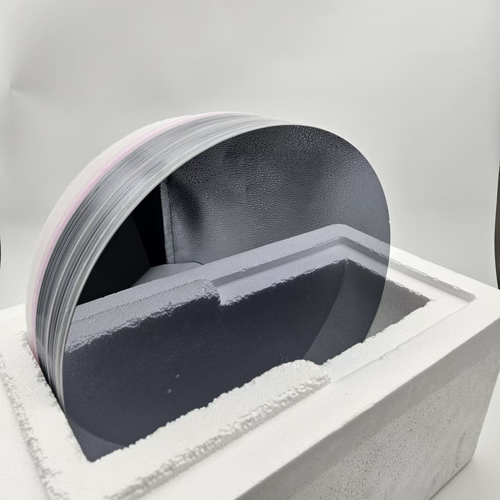
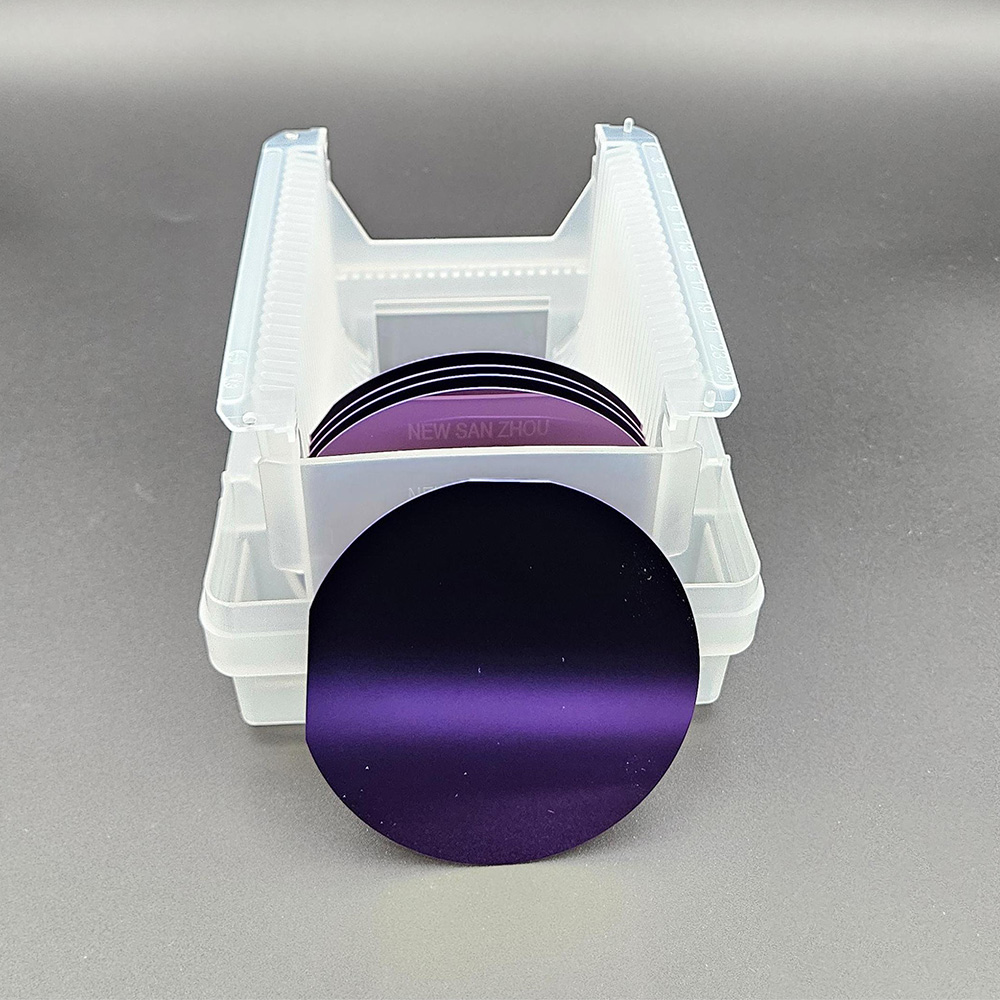
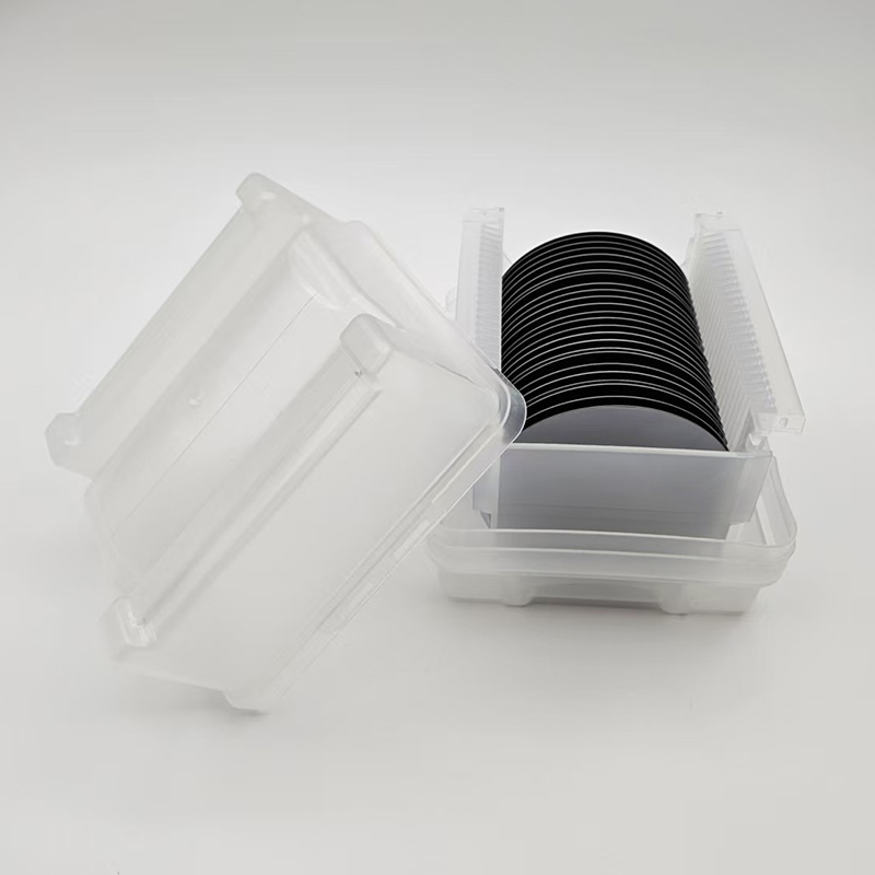
Packaging and Transportation
The packaging should be able to withstand the impact, vibration, stacking and extrusion that may be encountered during transportation, while also it has to easy to load, unload and handle.
We use professional wafer box packaging. The wafer box is protected by a double layer bag, the inside is a PE bag that can be dust-proof, and the outside is a aluminum foil bag that can be isolated from the air. The two-layer bags are vacuum-packed.
We will choose carton models according to different sizes of products. And between the product and the carton filled with shock-proof EPE foam, play a comprehensive protection.
Finally choose air transport to reach the customer's hands. This allows customers in any country and region to receive the product in the fastest time.
We comply with the Material Safety Data Sheet (MSDS) rules to ensure that the products transported are free of harmful substances and will not cause environmental pollution and explosion and other possible hazards.

Enterprise Strength
Factory Area: 3000 sq
Process:
1. Shaping→2. Edge Profile→3. Lapping→4. Polishing→5. Cleaning→6. Packing→7. Transportation
Capacity:
Glass Wafer --- 30K pcs
Silicon Wafer --- 20K pcs
(Equal to 6in)

Quality Assurance
Quality inspection method: Product inspection in accordance with SEMI standard or according to customer's requirements, together with product COA.
Warranty period: In accordance with the contract requirements.
Quality system management:
●Organize production according to ISO9001 and other quality system standards.
Quality management system and measures:
●Establish a strict quality assurance system, the heads of all departments and quality engineers to ensure the coordinated operation of the quality system.
●Strengthen the quality inspection system, strengthen the process quality control
●Strict material quality control, ensure that the input materials meet the design requirements and technical specifications.
●Implement a timely filing system for technical data to ensure that all processing technical data is complete/accurate.
Quality control in the production stage:
●Production preparation stage: carefully organize relevant personnel to learn product drawings and technical rules, and improve the technical level of employees.
●Quality control of the production process: the implementation of a strict handover system, the previous step of the process to the next step of the transfer, should be detailed processing. At the same time, strengthen the quality inspection system to ensure the quality of each step of the process.
●Quality acceptance: All processes must be quality acceptance before proceeding to the next process.

Pre-sales and After-sales
Pre-sales Service
Professional technical support and commercial team to help you determine product specifications according to product use, and issue specifications.
On-purchase Service
Produce products according to the confirmed specifications and our process.
After Sale Service
We will respond to any product problems encountered by customers or process problems encountered by customers within 24 hours. We can choose from various forms of service, such as email, video conference and so on.
Plutosemi Co., Ltd. was established in 2019, headquartered in Nanhai, Foshan, focusing on the research and development, production, and sales of high-performance semiconductor materials.
Advanced production capacity: We have three major production bases in China, with a monthly production capacity of 100000 equivalent 6-inch silicon wafers and 30000 equivalent 8-inch glass wafers, ensuring stable and efficient product supply for our customers.
High quality products: We provide efficient and stable product supply innovative solutions in the fields of glass wafers, silicon polishing wafers, epitaxial wafers (EPI), silicon on insulator wafers (SOI), and more. Our silicon wafers have the characteristics of ultra-thin, ultraflat, and high-precision, which can meet the needs of various high-end applications. Our glass and quartz substrates are also renowned for their high smoothness and precise aperture design.