


PlutoSemi High-Resistivity Silicon Wafers: Enabling High-End Applications in Silicon Photonics, RF, and Precision Sensing
With the explosive growth in demand for high-speed optical interconnects driven by AI computing clusters, the continuous evolution of automotive millimeter-wave radar toward higher frequency bands, and the ongoing improvement of industrial and aerospace-grade MEMS sensing accuracy, semiconductor substrate materials located at the upstream of the industry chain have become a key factor determining the performance limits of devices. Limited by carrier concentration, conventional doped Silicon Wafers generally suffer from high leakage current, significant signal loss, and noticeable optical absorption in high-frequency, optoelectronic integration, and precision sensing applications, making them difficult to support the design requirements of advanced devices. The high-resistivity silicon wafers developed by Plutosemi Co., Ltd. feature three core advantages: low leakage characteristics similar to insulation, no RF loss, and low optical absorption, providing stable and reliable substrate solutions for silicon photonic PIC, millimeter-wave RF, high-precision inertial sensors, and pressure sensing applications.
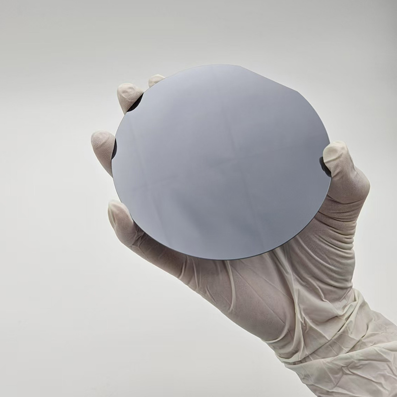
For highly integrated semiconductor devices, substrate leakage current and parasitic crosstalk are key factors restricting integration density and signal-to-noise ratio. Conventional silicon wafers have relatively low resistivity, allowing conductive paths to form between devices through the substrate, resulting in parasitic capacitance and leakage current. This not only increases unnecessary power consumption but also causes signal interference, leading to reduced device performance.
PlutoSemi high-resistivity silicon wafers achieve near-insulating substrate characteristics through extremely low carrier concentration, effectively cutting off parasitic conduction paths between devices and significantly reducing leakage current and crosstalk levels. This characteristic not only improves the overall signal-to-noise ratio of chips but also supports higher-density device layouts, providing more design flexibility for complex integrated chips, especially for precision analog circuits and sensor devices that are highly sensitive to leakage.
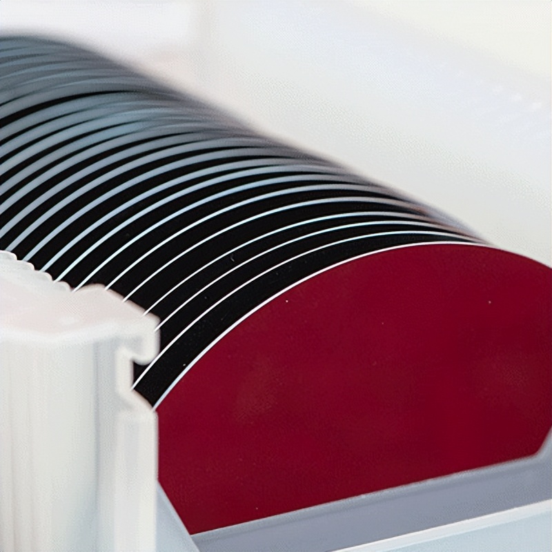
At millimeter-wave and even terahertz frequency ranges, conventional silicon substrates generate significant RF losses: high-frequency electromagnetic waves penetrate through the oxide layer into the silicon substrate, where they induce eddy currents inside the conductive substrate. This converts signal energy into heat loss while also causing signal distortion and a decrease in quality factor (Q value), directly limiting the operating frequency and performance ceiling of RF devices.
PlutoSemi high-resistivity silicon wafers, with their ultra-high resistivity, greatly suppress eddy current effects inside the substrate, reducing RF insertion loss to an extremely low level. At the same time, they weaken nonlinear effects caused by parasitic surface conductivity at the SiO₂-Si interface. When applied to RF devices, they can significantly improve the Q value of on-chip inductors, filters, phase shifters, and other passive components, reduce signal distortion and crosstalk, ensure signal integrity and stability in millimeter-wave frequency bands, and meet the strict requirements of high-frequency applications such as 5G/6G communications and automotive radar.
In silicon photonic integrated circuit (PIC) chips, the optical absorption of substrate materials in operating wavelength ranges is an important factor affecting optical signal transmission efficiency. Conventional silicon wafers have high free carrier concentrations inside the material, which can cause photon absorption in near-infrared and other operating wavelength ranges, resulting in optical signal attenuation, increased noise, and reduced transmission distance and bandwidth of optical links.
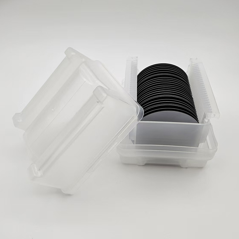
PlutoSemi high-resistivity silicon wafers significantly reduce optical losses caused by carrier absorption by reducing the number of free carriers inside the crystal, allowing optical signals to transmit more stably through waveguide structures above the substrate. This characteristic effectively improves the optical link efficiency of silicon photonic chips, reduces device noise, provides material support for the performance improvement of high-speed optical modulators, photodetectors, and photonic integrated circuits, and meets the application requirements of CPO co-packaged optics and high-speed optical modules in data centers.
Based on these three core performance advantages, PlutoSemi high-resistivity silicon wafers are deeply adapted to three major high-end fields: silicon photonic PIC, millimeter-wave RF, and high-precision MEMS sensing. They cover the entire process requirements from R&D verification to mass production. The products are available in full-size specifications from 2 to 8 inches and support various surface treatment methods to meet the processing requirements of different production lines.
Against the backdrop of intensifying global semiconductor industry competition and the urgent demand for independent control of high-end materials, breakthroughs in domestic substrate materials are of great significance. PlutoSemi has been deeply engaged in the silicon wafer material field. Relying on mature float-zone crystal growth technology and precision processing capabilities, the high-resistivity silicon wafers developed by PlutoSemi have reached advanced industry levels in key indicators such as resistivity uniformity, surface flatness, and impurity control.
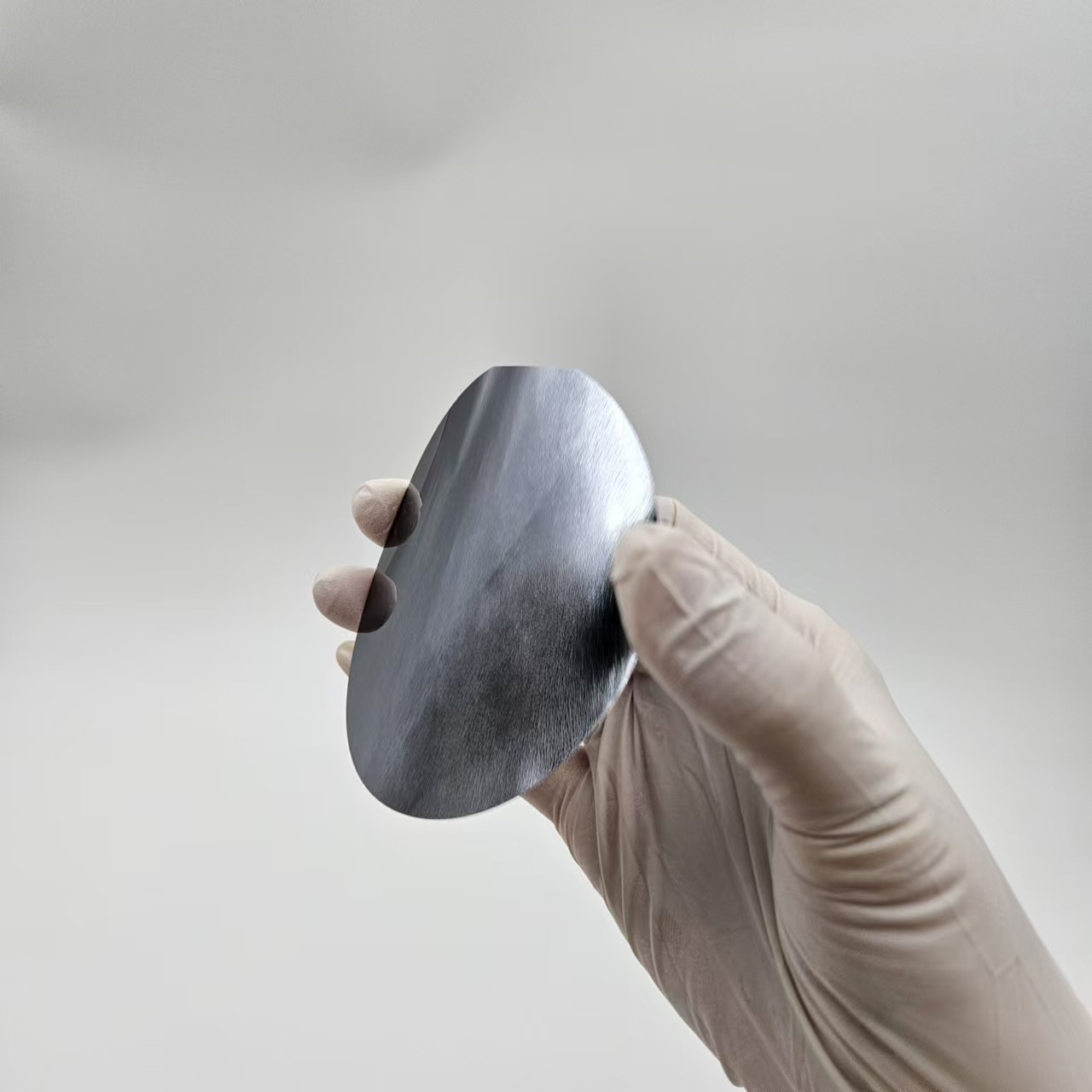
From the high-speed interconnection of silicon photonic chips, to the precise sensing of millimeter-wave radar, and the reliable measurement of precision sensors, PlutoSemi high-resistivity silicon wafers are serving as core foundational materials to support the technological evolution and mass production implementation of advanced downstream devices.
In the future, with the continuous emergence of more high-end application scenarios, PlutoSemi will continue to optimize material performance and process capabilities, providing solid substrate support for the high-quality development of China’s semiconductor industry.