


PlutoSemi Secures Hundreds of Thousands of Silicon Wafer and Glass Wafer Orders from German Customers
PlutoSemi Achieves New Milestone in Global Semiconductor Materials Market
Recently, Plutosemi Co., Ltd. (International brand: PlutoSemi), a domestic semiconductor materials company, has reached a long-term procurement agreement with a well-known German company. The German customer will purchase Silicon Wafer and Glass Wafer products from PlutoSemi, with an annual procurement volume reaching hundreds of thousands of pieces. This cooperation marks another significant improvement in PlutoSemi’s competitiveness in the global high-end semiconductor materials market.
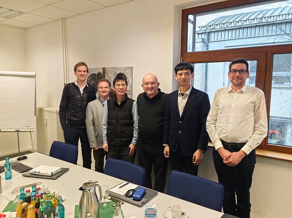
Germany, as a core hub of the European semiconductor industry, gathers world-leading manufacturing capabilities in automotive chips, industrial sensing, optical communications, and MEMS sensors. The country applies European Union standards for wafer substrate requirements, including material purity, surface microstructure, thermomechanical compatibility, and batch-to-batch consistency. PlutoSemi’s product specifications have successfully passed customer production line certification, securing a stable annual procurement volume of hundreds of thousands of wafers, with continuous production scheduling and delivery.

Customer Recognition of PlutoSemi’s Product Quality and Manufacturing Capabilities
A representative from the German customer stated:
“After multiple rounds of validation and small-batch trial production, we confirmed that PlutoSemi’s products have fully reached the level of international first-tier suppliers in terms of crystal defect control, electrical performance consistency, and batch stability. At the same time, relying on its fully integrated independent production lines in the Greater Bay Area of China, PlutoSemi can provide more flexible customized services and shorter delivery cycles. This is the core reason why we chose to establish an annual procurement agreement of hundreds of thousands of pieces.”

Advanced Manufacturing Capabilities Supporting High-End Semiconductor Applications
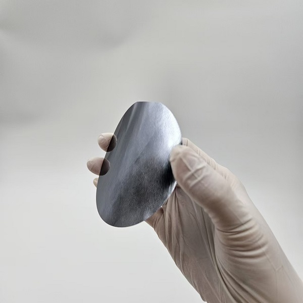
As one of the few manufacturers in South China capable of simultaneously completing fully customized silicon wafer and glass wafer processes, PlutoSemi relies on its own 4,000-square-meter production facility to build Class 1,000 and Class 100 cleanroom environments.
The company strictly controls temperature and humidity within ±0.5℃, air pressure differences, and dust particles to meet the mirror polishing, micro-processing cleanliness, and precision manufacturing requirements of optical glass wafers, ultra-thin silicon wafers, and TGV through-hole substrates.
Dedicated clean areas for silicon wafers and glass wafers are separated to prevent cross-contamination between the two substrate materials and ensure stable processing yields. PlutoSemi has established complete in-house production lines covering grinding, CMP polishing, femtosecond laser TGV, cutting and chamfering, fully automatic wet cleaning, and precision inspection.
All equipment is independently controlled and production scheduling is managed internally, eliminating delays caused by outsourcing transfers and ensuring consistency in process standards. For urgent customized samples, PlutoSemi can activate dedicated equipment priority channels to significantly shorten delivery cycles.
Previously, the company has already maintained stable supply relationships with multiple leading domestic semiconductor companies and research institutions, including Huawei, Xinkailai, Shanghai Xinxin, Pindun Technology, Sunny Optical, Crystal-Optech, and other representative enterprises in the industry.
Supporting the Global Expansion of Semiconductor Substrate Manufacturing
The head of PlutoSemi’s overseas business division stated that the implementation of the German customer’s annual procurement order of hundreds of thousands of wafers represents authoritative recognition from the international high-end market of China’s precision processing capabilities for wafer substrates, mass production consistency, and full-process supporting service systems.
This cooperation represents a milestone event in which China’s semiconductor substrate industry is moving from “domestic substitution” toward “global supply.”
In the future, PlutoSemi will continue increasing investment in R&D, improving production capacity and process capabilities, and providing higher-quality semiconductor material solutions for global customers.