


PlutoSemi High-Resistivity Silicon Wafers: Enabling High-End Applications in Silicon Photonics, RF, and Precision Sensing
A Professional Manufacturer Providing Integrated Silicon and Glass Wafer Solutions
Recently, Plutosemi Co., Ltd. (International brand: PlutoSemi), located in Wanma (Intelligent Manufacturing) Industrial Park, Gaoming District, Foshan, Guangdong-Hong Kong-Macao Greater Bay Area, has continued to release industrial growth momentum. Relying on its own full-process wafer processing production lines, dual-substrate simultaneous manufacturing capabilities, and strict clean production systems, the company has established integrated service capabilities covering Silicon Wafer and glass wafer R&D, customized processing, and chip foundry services. Its products are exported to multiple regions worldwide, with exports accounting for more than 50%. PlutoSemi has become one of the rare professional manufacturers in South China with large-scale customized production capabilities for both silicon-based and glass-based advanced substrates, helping achieve independent and controllable supply chains for critical semiconductor substrate materials.
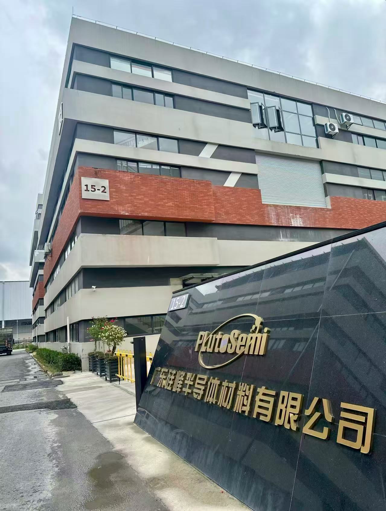
Advanced Manufacturing Facilities and High-Purity Production Environment
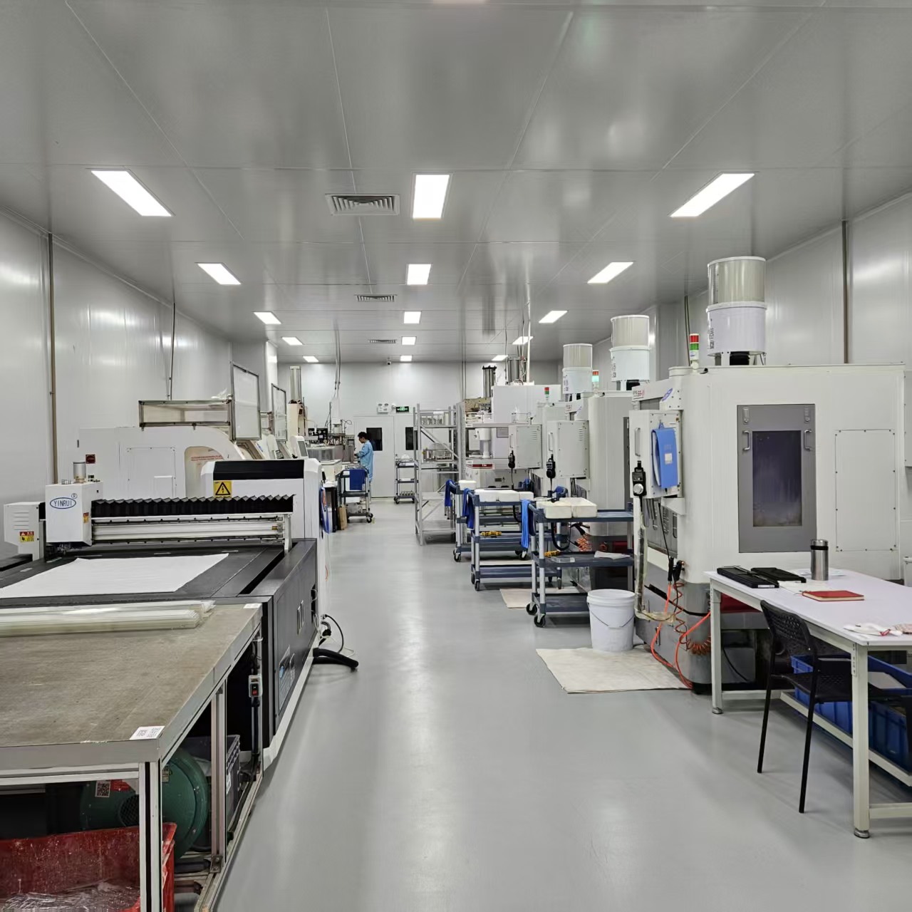
PlutoSemi’s factory covers a total construction area of more than 4,000 square meters and features a classified clean production environment, including a 1,000-square-meter Class 1,000 cleanroom and a 200-square-meter Class 100 cleanroom. The facility is designed to meet high-cleanliness precision processing requirements such as mirror polishing, ultra-thin wafers, and TGV through-holes. Located near the under-construction Pearl River Delta Hub (Guangzhou New) Airport, the factory provides convenient logistics access to domestic and international markets.
Strong Technical Accumulation and Wide Application Coverage
After years of technological development, the PlutoSemi team has obtained more than 20 patents related to silicon wafer and glass wafer substrates, forming a comprehensive product and foundry service system. The company’s production capacity continues to steadily increase, currently reaching an equivalent 6-inch capacity of 30,000 silicon wafers per month and 50,000 glass wafers per month.
Its products are widely used in advanced fields including semiconductor chips, optical communications, AR/VR optical displays, inertial/pressure/gas MEMS sensors, and gene sequencing medical biotechnology. PlutoSemi has established stable supply relationships with leading domestic companies and key research institutions, including Huawei, Xinkailai, Shanghai Xinxin, Pindun Technology, Sunny Optical, Crystal-Optech, and other industry-leading enterprises.
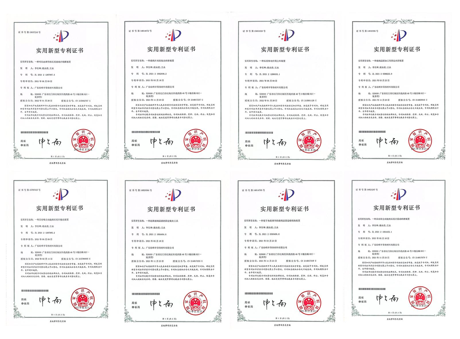
Leveraging the Greater Bay Area Semiconductor Ecosystem
Relying on the complete semiconductor industrial ecosystem in the Greater Bay Area and being close to semiconductor design, MEMS sensing, optical technology, and new energy vehicle electronics clusters in Shenzhen and Guangzhou, PlutoSemi provides advantages including nearby factory visits, on-site process communication, and rapid sample delivery for customers in surrounding regions.
The company actively expands global markets, with its business coverage including Mainland China, Hong Kong, Taiwan, Singapore, Vietnam, Japan, South Korea, India, the United States, Germany, France, the United Kingdom, Russia, and other countries and regions.
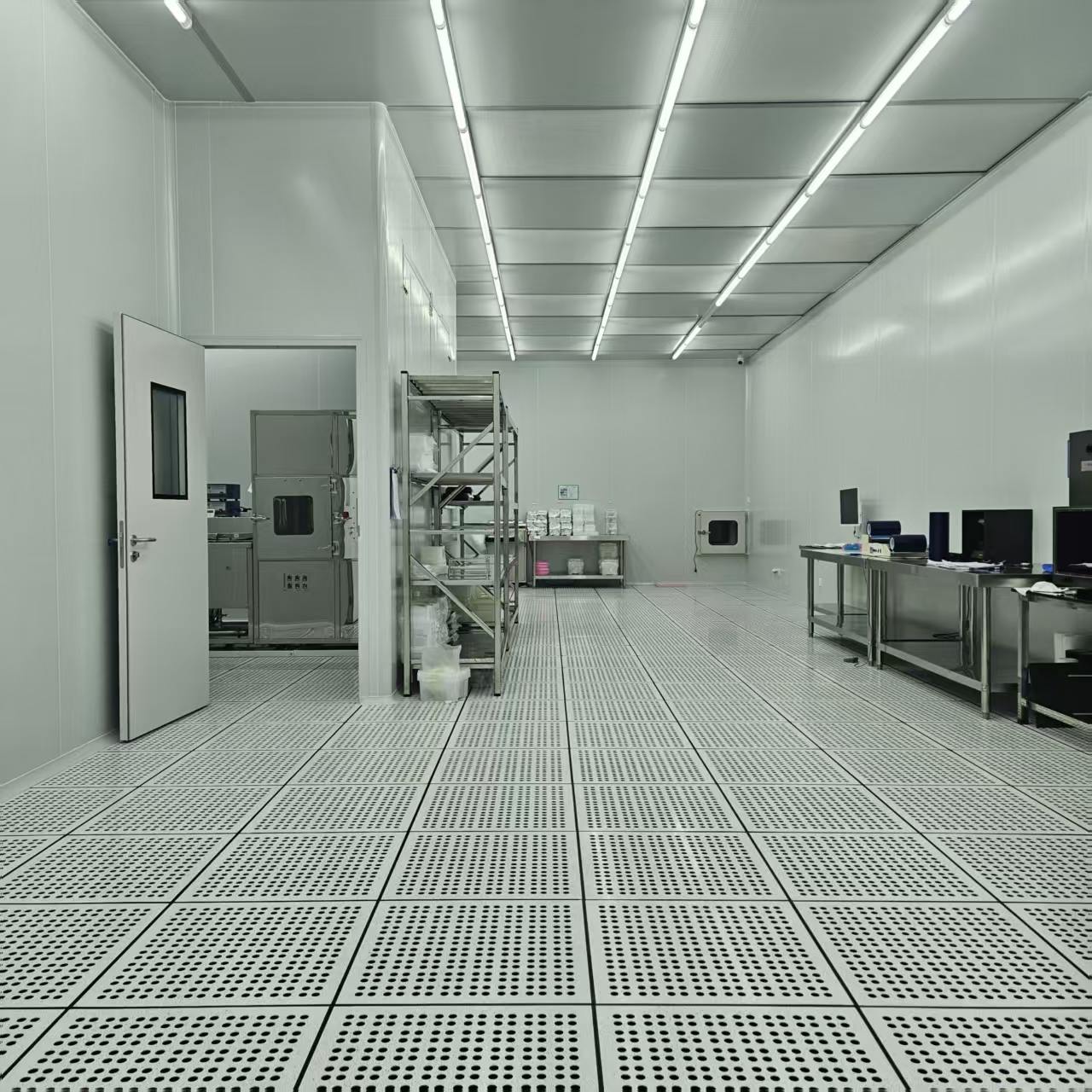
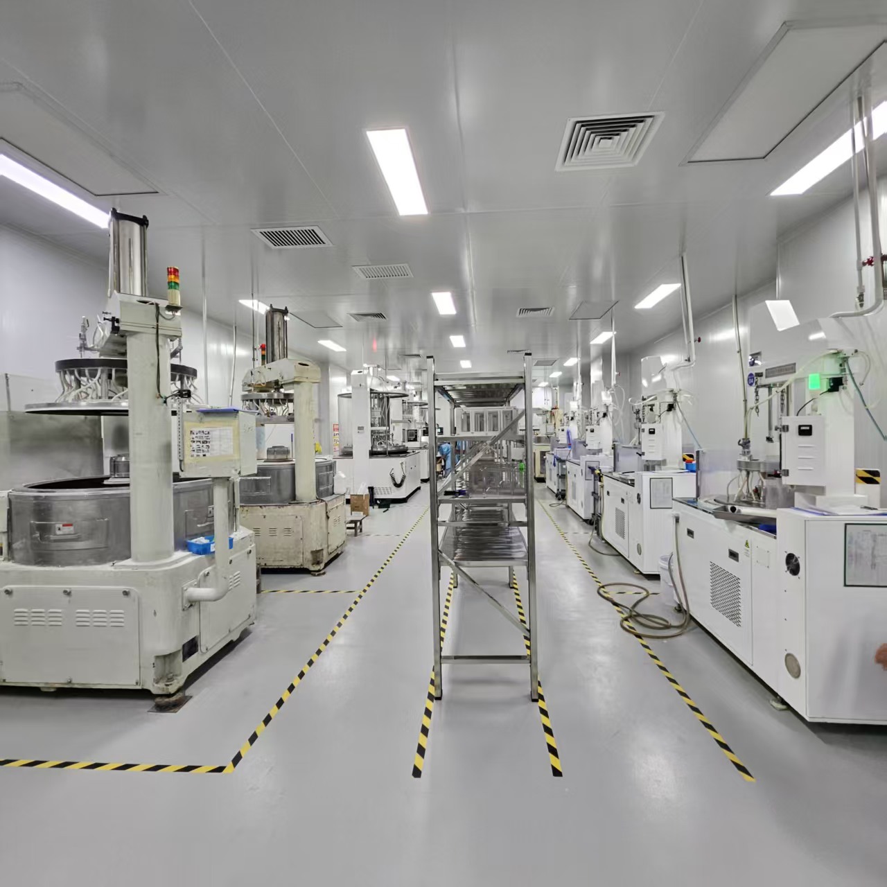
Complete In-House Production and Precision Processing Capabilities
At the same time, PlutoSemi has established a complete independent production line covering grinding, CMP polishing, femtosecond laser TGV, cutting and chamfering, fully automatic wet cleaning, and precision inspection.
Core equipment includes wafer cutting machines, CNC precision engraving machines, single-sided and double-sided precision grinding machines, chemical mechanical polishing equipment, multi-station cleaning integrated machines, SPM cleaning lines, and other advanced production equipment.
The company is also equipped with a complete range of precision inspection instruments, including wafer type testing equipment, resistivity testers, crystal orientation analyzers, particle inspection equipment, interferometers, and other testing systems. All equipment is independently controlled and production scheduling is managed internally, with no outsourcing transfer processes, fundamentally ensuring consistency of process standards and controllability of delivery efficiency.
Flexible One-Stop Customization Services for Semiconductor Substrates
To meet the increasingly personalized requirements in the semiconductor substrate field, PlutoSemi has established a one-to-one customized service system covering the entire process from “drawing confirmation → process sampling → parameter adjustment → sample retesting → mass production.”
The company supports comprehensive non-standard customization services including size, thickness, surface roughness, polishing grade, slotting, drilling, edge chamfering, coating pre-treatment, special crystal orientation, and customized-shaped wafers.
It supports both small-batch R&D samples and stable mass production supply. Each customer is equipped with dedicated business and process engineers for direct communication. Customized solutions are retained exclusively, allowing future repeat orders without repeated confirmation of basic requirements, significantly reducing trial-and-error costs and communication costs during new product development.
Empowering Global Semiconductor Innovation Through Reliable Substrate Solutions
Looking ahead, PlutoSemi will continue to focus on the silicon wafer and glass wafer substrate segments. Guided by the corporate spirit of “full of ambition, perfect in details,” the company will continuously expand product boundaries and technological depth.
By further leveraging its geographical advantages and production capacity advantages, PlutoSemi will continue to empower global semiconductor innovation and development through highly flexible customization services, rapid response systems, and stable and reliable quality assurance.