


PlutoSemi Heavily Doped Low-Resistivity Silicon Wafers Pave the “Superconducting” Path for Power Devices
Heavily Doped Low-Resistivity Silicon Wafers Become a Key Foundation for Power Semiconductor Development
With the rapid growth of AI server computing, the upgrading of new energy vehicle power systems, and the widespread adoption of fast-charging terminals, power semiconductors, as core components for energy conversion and transmission, directly determine the operating efficiency limits of entire systems.
As the core substrate material for power chips, heavily doped low-resistivity silicon wafers have long exceeded the basic characteristics of conventional silicon wafers. They have become a key factor influencing device conduction loss, heat dissipation capability, and long-term reliability.
As a professional semiconductor material supplier, the heavily doped low-resistivity silicon wafers developed by Plutosemi Co., Ltd. (International brand: PlutoSemi) represent an important practitioner of this technological route.
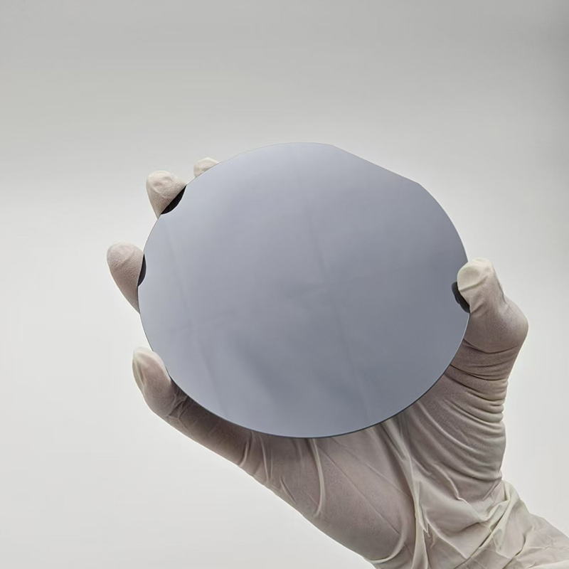
Ultra-Low Resistivity Enables High-Power and High-Frequency Applications
Unlike conventional lightly doped silicon wafers that can only meet the basic requirements of ordinary chips, PlutoSemi heavily doped low-resistivity silicon wafers use ultra-high concentration precision doping technology to reduce wafer resistivity to an extremely low level.
This effectively addresses industry challenges such as excessive heat generation, high power loss, unstable contact performance, and poor heat dissipation in high-power and high-frequency operating scenarios.
These wafers are widely used in several key applications, including MOS/IGBT epitaxial substrates, fast-charging power transistors, heating-type gas MEMS, and power transfer carriers.
IGBTs and power MOSFETs are core switching devices used in new energy vehicles, industrial frequency conversion systems, and energy storage converters.
These devices commonly adopt the classic structure of “heavily doped substrate + epitaxial layer.” PlutoSemi heavily doped low-resistivity silicon wafers, as the core bottom substrate, can provide a flat and defect-free foundation for epitaxial processes, ensuring epitaxial layer growth quality.
At the same time, their ultra-low resistance characteristics create efficient vertical high-current channels, significantly reducing the overall conduction voltage drop of devices.
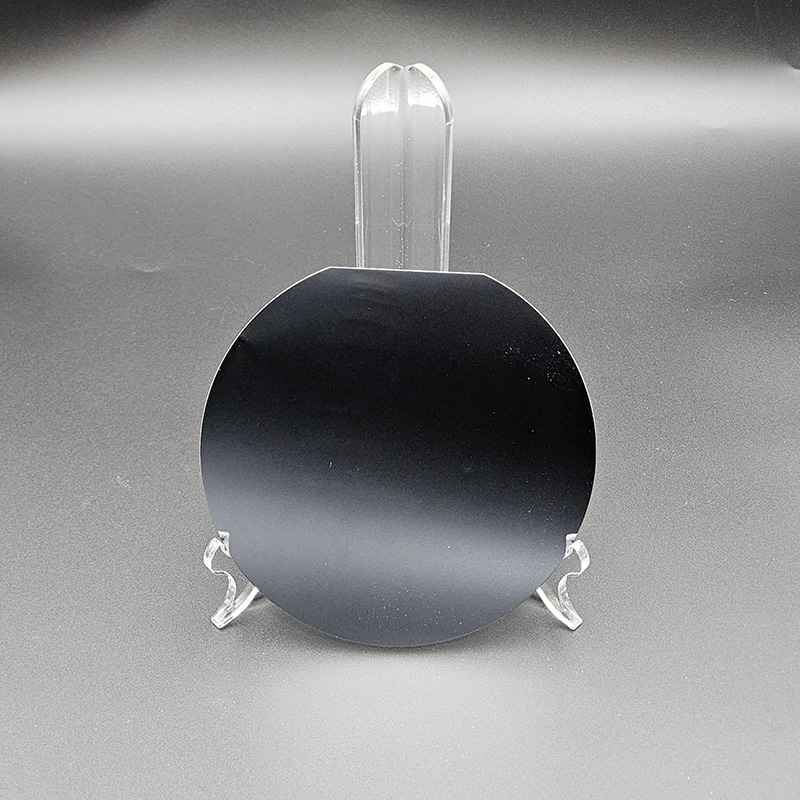
Core Material Supporting Next-Generation Power Electronics
With nearly metal-like electrical conductivity, extremely low conduction loss, excellent ohmic contact performance, and outstanding heat dissipation capability, heavily doped low-resistivity silicon wafers have become an indispensable core material in the power semiconductor industry chain.
From MOS/IGBT epitaxial substrates to fast-charging power transistors, from MEMS gas sensors to power transfer carriers, heavily doped low-resistivity silicon wafers are providing solid material support for innovation and development in next-generation power electronics, artificial intelligence, new energy vehicles, and intelligent sensing fields.
PlutoSemi Provides High-Performance Customized Heavily Doped Low-Resistivity Silicon Wafers
PlutoSemi’s factory covers more than 4,000 square meters and features standardized clean production workshops, including a 1,000-square-meter Class 1,000 cleanroom and a 200-square-meter Class 100 cleanroom.
The company has mastered core processes including mature high-concentration precision doping, high-precision polishing, and flatness control, enabling stable production of heavily doped low-resistivity silicon wafers with uniform electrical performance, extremely low defect rates, and qualified cleanliness levels.
PlutoSemi supports customized production in mainstream sizes of 2/4/6/8/12 inches and can accurately adjust resistivity, wafer thickness, and oxide layer parameters according to customer requirements to meet different device process demands.
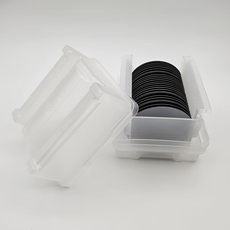
Supporting semiconductor supply chain Independence Through Localized Manufacturing
For a long time, high-end heavily doped low-resistivity silicon wafers in China have relied heavily on imports, facing challenges such as unstable supply chains, long delivery cycles, and high costs.
PlutoSemi heavily doped low-resistivity silicon wafers combine the advantages of localized customization, rapid delivery, and high adaptability, effectively solving critical industry bottlenecks and supporting the independent development and high-quality growth of China’s semiconductor industry chain.
With the continuous improvement of requirements for power density and energy efficiency in advanced applications such as AI servers, high-voltage fast charging, and smart grids, the technological evolution and market opportunities of heavily doped low-resistivity silicon wafers will continue to expand.
Professional companies such as PlutoSemi, which are deeply engaged in the semiconductor materials field, will play an increasingly important role in this development process.