


PlutoSemi TGV Glass Wafers Build the Foundation for Semiconductor Optoelectronic Packaging
TGV Glass Wafers Become a Key Substrate Material for Advanced Optoelectronic Packaging
With the explosive growth of AI computing demand, accelerated deployment of 5G/6G communications, and the large-scale commercialization of AR/VR displays, glass substrates, with their low dielectric loss, adjustable coefficient of thermal expansion, and excellent optical properties, are gradually replacing traditional organic substrates and silicon substrates to become core carriers for optoelectronic packaging.
As one of the few professional manufacturers capable of simultaneously completing fully customized Silicon Wafer and glass wafer processes, Plutosemi Co., Ltd. (International brand: PlutoSemi) relies on its own femtosecond laser TGV production line to provide suitable glass wafer solutions for application scenarios including AR/VR micro-display chip TGV packaging substrates, CPO co-packaged optical photonic engine interposers, and optical communication transceiver chip packaging substrates.
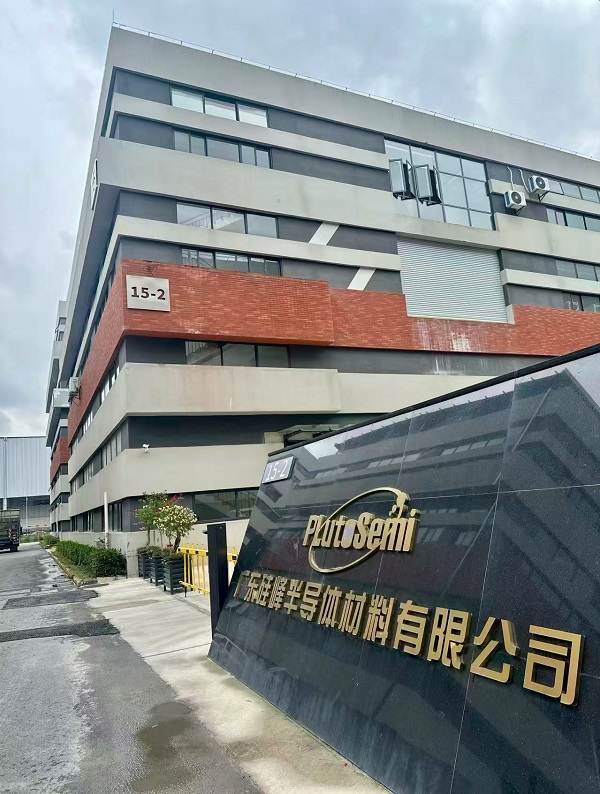
TGV Glass Wafers Empower AR/VR Micro-Display Chip Packaging
AR/VR near-eye display devices place extremely high requirements on packaging substrates for micro-display chips, including ultra-thin design, high flatness, low power consumption, and high-density interconnection.
Traditional PCB substrates are prone to warping in ultra-thin applications, have insufficient heat dissipation capabilities, and face limitations in regional precision. PlutoSemi’s femtosecond laser TGV through-glass via wafers, with higher flatness, lower power consumption, and lighter characteristics, have become an ideal packaging carrier for Micro LED micro-display chips.
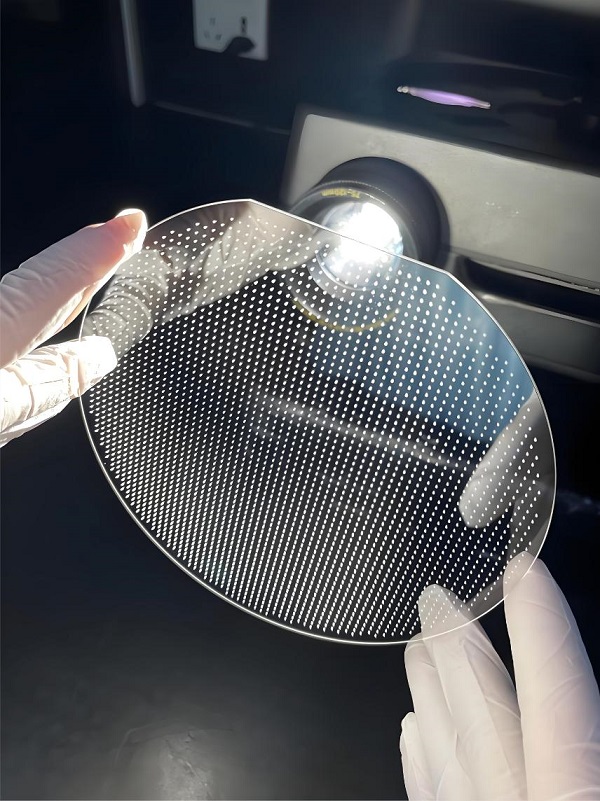
TGV Glass Wafer Solutions Support CPO Optical Packaging Applications
Co-packaged optics (CPO) technology integrates optical engines and electrical chips into a single package, using light instead of electricity for data transmission between chips. It is a key solution for meeting the high-bandwidth and low-power interconnection requirements of data centers and AI clusters.
The CPO photonic engine interposer, as the core carrier for optoelectronic signal conversion and transmission, places strict requirements on the material’s high-frequency electrical performance, signal integrity, and thermal management capabilities.
For this reason, PlutoSemi provides high-resistivity TGV glass wafers, with their core advantages being particularly prominent in high-frequency applications.
Excellent insulation properties enable high-density integration. As a naturally insulating material, high-resistivity glass does not require additional insulation layer deposition on the inner walls of through holes, enabling vertical interconnection while significantly simplifying manufacturing processes and reducing production costs.
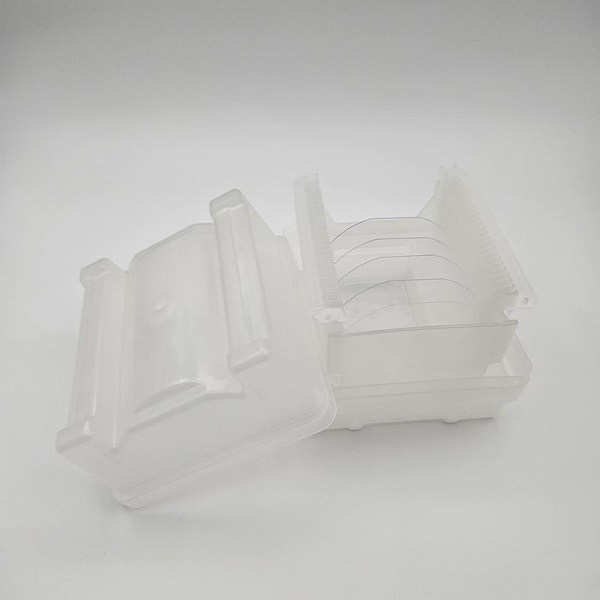
Borosilicate TGV Glass Wafers Improve High-Frequency Optical Communication Packaging
Optical communication transceiver chips are key components for data center interconnections and 5G front-haul/backhaul networks. Their packaging substrates need to achieve a balance between high-frequency transmission performance, thermal stability, and cost control.
Traditional organic substrates experience relatively high losses during high-frequency transmission, while silicon interposers face challenges in terms of cost.
Borosilicate TGV glass wafers are currently one of the most widely used substrate materials in TGV processes. Their characteristics are highly compatible with optical communication transceiver chip packaging requirements.
The excellent dielectric properties of borosilicate glass ensure high-frequency signal transmission. Its low dielectric constant and low loss characteristics can significantly reduce substrate losses and parasitic effects during high-frequency signal transmission.
During laser-induced etching processes, borosilicate glass demonstrates excellent processing consistency. A single wafer needs to integrate millions or even tens of millions of metallized through-holes, and the maturity and mass production capability of borosilicate glass TGV processes have been widely validated by the industry.
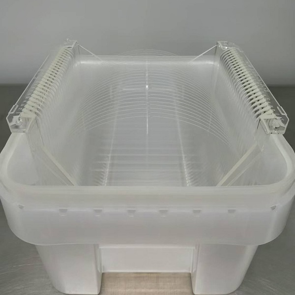
PlutoSemi Provides Flexible Customized Glass Wafer Solutions
In its glass wafer product line, PlutoSemi provides glass wafers, silicon polished wafers, epitaxial wafers (EPI), silicon-on-insulator wafers (SOI), and other glass-based materials.
The company supports comprehensive non-standard customization services including thickness, surface roughness, polishing grade, slotting, drilling, edge chamfering, coating pre-treatment, special crystal orientation, and customized-shaped wafers.
The solutions are compatible with both small-batch R&D sampling and stable mass production supply.
Currently, PlutoSemi’s glass wafer production capacity has reached an equivalent of 50,000 6-inch wafers per month. Its products are exported to multiple regions worldwide and have been stably supplied to leading domestic industry companies and research institutions, including Huawei, Xinkailai, Shanghai Xinxin, Pindun Technology, Sunny Optical, and Crystal-Optech.
The company has also obtained annual procurement orders of hundreds of thousands of silicon wafers and glass wafers from a well-known German enterprise, marking authoritative recognition from the international high-end market for China’s precision glass wafer processing capabilities.
Driving the Evolution of High-End Optoelectronic Packaging Materials
In the future, PlutoSemi will continue to focus on the technological evolution of glass wafers, concentrating on improving through-hole yield, optimizing wafer precision, expanding product specifications, and continuously enhancing its high-end optoelectronic packaging material product portfolio.