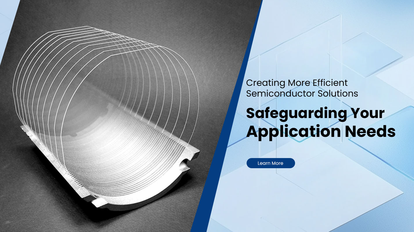
How to Cut Silicon Wafer?
Cutting Silicon Wafers is one of the most delicate and crucial steps in semiconductor manufacturing. Precision in this stage directly affects the performance, yield, and integrity of microelectronic devices. Silicon wafers, typically ranging from 100 mm to 300 mm in diameter, are extremely thin and brittle, requiring specialized equipment, environmental control, and optimized cutting parameters to achieve clean, crack-free edges. Understanding the right cutting methods and preparation procedures is key to maintaining wafer quality while maximizing production efficiency.
Understanding the Structure of Silicon Wafers
Silicon wafers are thin slices of single-crystal silicon grown through the Czochralski or Float-Zone process. Their surfaces are precisely polished to atomic-level smoothness before being processed into chips. The crystal structure is highly ordered, which gives silicon its semiconducting properties but also makes it prone to chipping when exposed to mechanical stress.
Before cutting, wafers are typically coated with protective films to prevent contamination and edge damage. Cleanroom handling and temperature stability are essential to avoid micro-cracks caused by thermal or mechanical shock.
Common Methods for Cutting Silicon Wafers
Different wafer sizes and production needs call for different cutting techniques. The main cutting methods include diamond saw dicing, laser dicing, and stealth dicing. Each offers unique advantages in speed, precision, and yield rate.
| Cutting Method | Cutting Principle | Advantages | Limitations |
|---|---|---|---|
| Diamond Saw Dicing | Uses a high-speed diamond blade to mechanically cut wafers | Precise control, low cost, widely used | Generates debris, potential for edge chipping |
| Laser Dicing | Focused laser beam ablates silicon along cutting lines | No mechanical stress, cleaner edges | May cause localized heating |
| Stealth Dicing | Laser penetrates inside wafer to create internal cracks, then separates layers | Minimal debris, faster throughput | High equipment cost, requires advanced control |
Diamond Saw Dicing
This traditional method uses a rotating diamond-coated blade operating at speeds above 20,000 RPM. A constant flow of deionized water cools the wafer and removes debris. The cutting width, known as the kerf, is typically around 30–50 µm. Adjusting feed rate and spindle speed is essential to balance speed with surface integrity. Diamond dicing is still the industry standard for mass production due to its simplicity and versatility.
Laser Dicing
Laser dicing replaces the physical blade with a high-energy laser beam, which vaporizes the silicon along pre-defined scribe lines. The process eliminates mechanical contact, thus reducing edge cracks and particulate contamination. Infrared and ultraviolet lasers are commonly used depending on wafer thickness. Ultraviolet lasers (355 nm) are ideal for thin wafers below 100 µm because they produce minimal heat-affected zones.
Stealth Dicing
Stealth dicing is a more advanced, non-contact method in which a focused laser beam passes through the wafer’s surface and generates an internal modification layer. The wafer is then gently expanded, causing it to separate cleanly along the modified lines. This technique achieves excellent edge quality, eliminates slurry waste, and significantly improves yield. It is commonly used for ultra-thin wafers in high-performance microelectronics and MEMS devices.
Preparation Before Cutting
Preparation determines cutting quality. The wafer must be thoroughly cleaned and mounted on a carrier tape before processing. A typical preparation workflow includes:
Cleaning – Removing particles and residues using deionized water and surfactants.
Mounting – Attaching the wafer to a UV-sensitive adhesive film to prevent movement during cutting.
Alignment – Positioning the wafer according to its crystal orientation (usually <100> or <111> plane).
Environmental Control – Maintaining humidity and temperature stability to reduce stress-induced cracking.
High-quality adhesive tapes with consistent tension ensure the wafer remains stable throughout the dicing process. The alignment system must recognize fiducial marks on the wafer to guarantee precise cutting paths.
Factors Influencing Cutting Quality
Several key factors directly affect the final quality and efficiency of wafer cutting:
Cutting Speed and Feed Rate: Higher feed rates improve productivity but may increase chipping. An optimized balance is crucial.
Blade Type or Laser Power: The correct diamond grit size or laser wavelength ensures clean edges and minimal thermal damage.
Cooling System: Continuous cooling prevents overheating and deformation. Deionized water or controlled airflow is typically used.
Vibration Control: Precision cutting machines must maintain micro-level stability to avoid fractures in the silicon lattice.
Cleanroom Environment: Dust and vibration can severely affect cut consistency and device yield.
Real-time monitoring of blade torque or laser energy helps maintain uniform performance and prevents tool wear from damaging the wafer.
Safety and Environmental Considerations
Wafer cutting involves fine silicon dust, slurry waste, and laser radiation. Proper ventilation, filtration systems, and protective shielding are necessary to maintain a safe and clean environment. Automated systems can collect debris and recycle cooling water to minimize waste. Modern production facilities also employ low-emission laser systems that reduce environmental impact without compromising precision.
Automation and Smart Cutting Solutions
As semiconductor devices become smaller and thinner, demand for high-precision, automated wafer cutting has grown. Advanced systems now integrate vision alignment, AI-based process control, and automatic tape expansion. These innovations not only enhance accuracy but also reduce material waste and operator dependency.
Plutosemi, a specialist in silicon wafer processing equipment, offers cutting solutions designed for high-precision applications. Their systems provide superior control over cutting depth, alignment, and surface cleanliness, helping manufacturers achieve faster throughput with minimal wafer loss. With a focus on precision engineering and consistent yield, Plutosemi’s equipment supports the evolving needs of semiconductor fabrication worldwide.
Conclusion
Cutting silicon wafers is a complex process requiring careful balance between speed, accuracy, and surface quality. Selecting the appropriate cutting technique — whether diamond saw, laser, or stealth dicing — depends on wafer thickness, material properties, and production goals. Proper preparation, environmental control, and equipment maintenance are essential for consistent results.
By integrating advanced dicing technologies and automation systems like those from Plutosemi, manufacturers can achieve cleaner edges, higher yields, and greater efficiency in wafer production. In the rapidly evolving semiconductor industry, precision cutting remains the foundation of technological innovation and manufacturing excellence.


