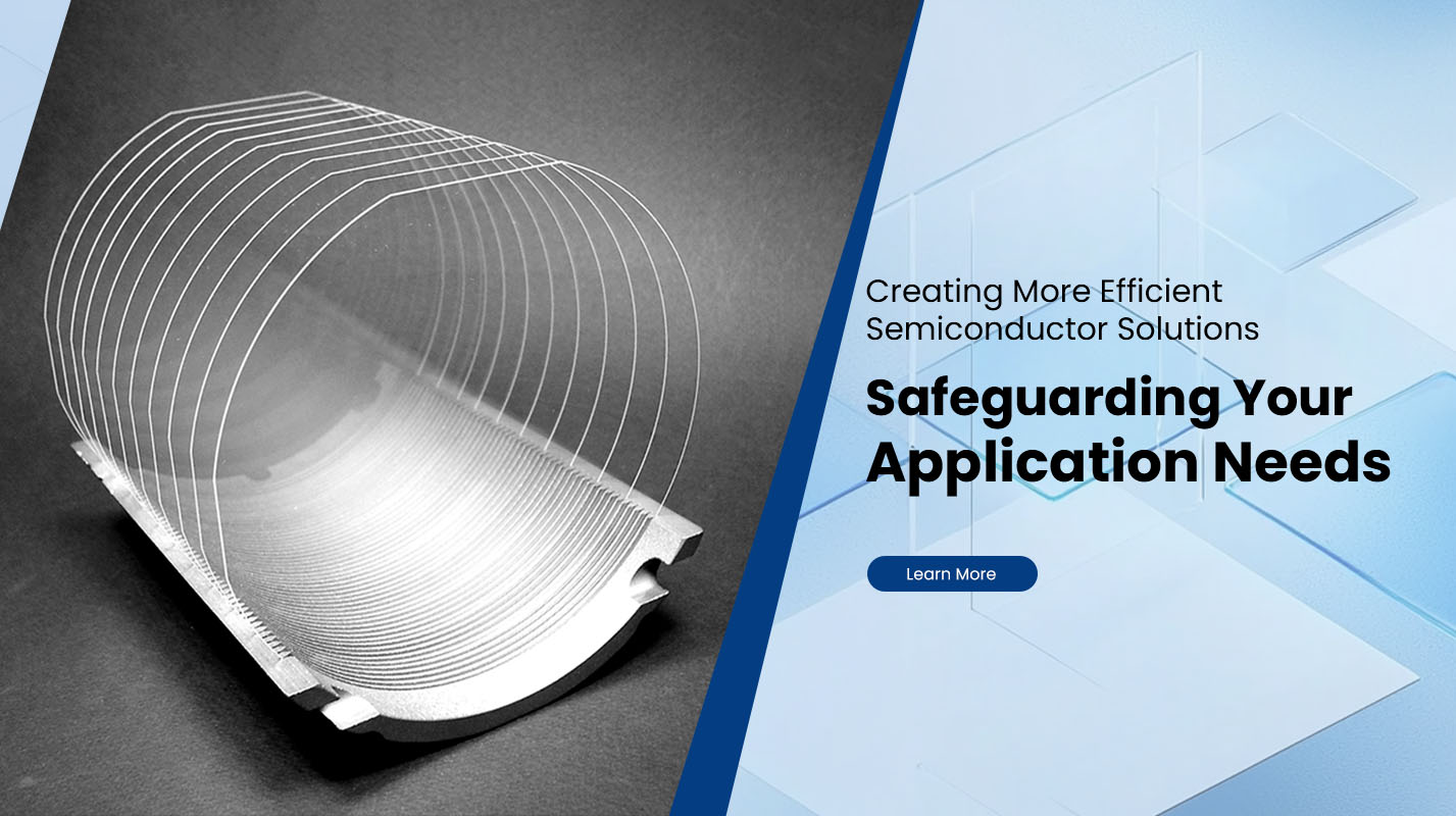
Silicon on Insulator, often abbreviated as SOI, is a semiconductor manufacturing technology in which a thin layer of silicon is separated from the bulk substrate by an insulating layer. This structure is different from traditional bulk silicon wafers because the active devices are formed on a very thin silicon film placed above an oxide layer.
-
2025-11-20
-
2025-11-19Through Silicon Via is a vertical electrical connection that passes completely through a silicon wafer, making it a key interconnect method in modern 3D integrated circuits and advanced packaging. It shortens signal paths, reduces power loss, and supports high-density stacking in semiconductor devices.
-
2025-11-18Through Glass Via technology is a microfabrication method used to create vertical electrical connections that pass directly through a glass substrate. It enables high-density interconnects, precise signal pathways, and improved thermal performance in advanced electronic packaging.
-
2025-11-14In the semiconductor manufacturing industry, the flatness of a wafer substrate is a critical parameter. Without excellent flatness, downstream processes such as lithography, thin-film deposition, chemical mechanical polishing (CMP), and bonding can suffer in terms of yield, uniformity, and reliability.
-
2025-11-13In semiconductor manufacturing, polishing of wafers plays a critical role. A well-executed polishing process ensures the surface and subsurface integrity of the wafer, which in turn supports high yields and robust device performance. However, defects during polishing can compromise flatness, introduce scratches, pits, or particles, and ultimately reduce reliability.
-
2025-11-12In advanced semiconductor packaging, the vertical interconnection through glass wafers known as Through Glass Via (TGV) technology is gaining prominence. Unlike traditional interconnects that rely on silicon or organic substrates, TGVs make use of glass substrates to form metallised vias that connect front and back of a wafer or interposer.
-
2025-11-11Epitaxial wafer growth refers to the process of depositing a crystalline film on a crystalline substrate such that the deposited film (the epitaxial layer) inherits the lattice structure and orientation of the underlying substrate. The result is a wafer in which the active semiconductor layer has been grown with very high crystalline quality.
-
2025-11-10Sapphire substrates, specifically single-crystal aluminium oxide (Al₂O₃) in wafer form, have become an indispensable material in advanced electronics, optoelectronics, and high-end optical components. Derived from the gemstone sapphire but grown in ultra-high-purity form, these substrates deliver a unique combination of optical transparency, electrical insulation, thermal performance, and mechanical robustness.
-
2025-11-08In the semiconductor industry, wafer thickness is a critical specification that directly influences mechanical strength, thermal performance, and device fabrication accuracy. A 6-inch silicon wafer, also known as a 150 mm wafer, is one of the most commonly used substrates in integrated circuit (IC) and MEMS manufacturing.
-
2025-11-07Cutting silicon wafers is one of the most delicate and crucial steps in semiconductor manufacturing. Precision in this stage directly affects the performance, yield, and integrity of microelectronic devices. Silicon wafers, typically ranging from 100 mm to 300 mm in diameter, are extremely thin and brittle, requiring specialized equipment, environmental control, and optimized cutting parameters to achieve clean, crack-free edges.
-
2025-11-06Sapphire substrates have become an essential foundation material in the semiconductor, optoelectronic, and photonics industries. Their exceptional physical and chemical stability make them ideal for manufacturing LEDs, laser diodes, RF devices, and optical components that demand extreme precision and durability.
-
2025-11-05In the semiconductor manufacturing industry, silicon wafers are the foundation upon which integrated circuits, microchips, and sensors are built. Among the various wafer sizes, the 300mm silicon wafer — equivalent to 12 inches in diameter — has become the industry standard for large-scale chip fabrication.


