


Australian Customers Visit PlutoSemi to Discuss Cooperation on Medical Testing Chip Processing
Australian Customers Visit PlutoSemi for Technical Exchange and Cooperation Discussion
On July 31, 2026, a delegation of Australian customers visited Plutosemi Co., Ltd. (International brand: PlutoSemi), toured PlutoSemi’s production lines and R&D manufacturing environment, and conducted in-depth discussions on medical testing chip manufacturing processes, processing capabilities, and the feasibility of future mass production.
This visit further strengthened both parties’ understanding of semiconductor precision processing technology applications and laid a solid foundation for future cooperation.
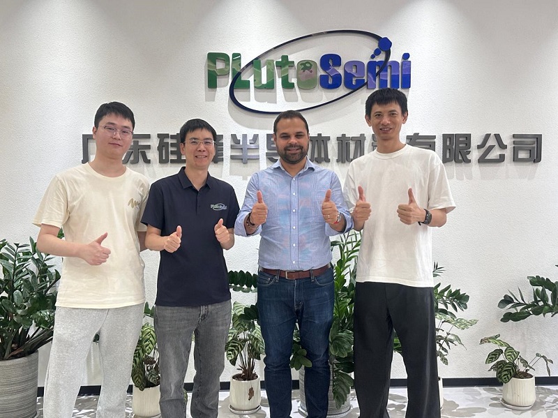
Exploring Advanced Semiconductor Processing Capabilities
During the visit, Australian customers entered PlutoSemi’s production workshop and gained detailed insights into the company’s manufacturing processes in areas including Glass Wafer processing, silicon-based and glass-based chip processing.
During the on-site communication, customers focused on production equipment configuration, process control, and product quality management systems, while gaining a deeper understanding of PlutoSemi’s technological accumulation and manufacturing capabilities in high-precision processing.
Through this visit, customers developed a more intuitive understanding of PlutoSemi’s complete capability system, covering material processing, process development, and large-scale manufacturing.
Subsequently, both parties conducted technical discussions regarding the medical testing chip project. The two technical teams carried out detailed communication on key aspects involved in chip manufacturing, including material selection, structural design, processing precision, and mass production.
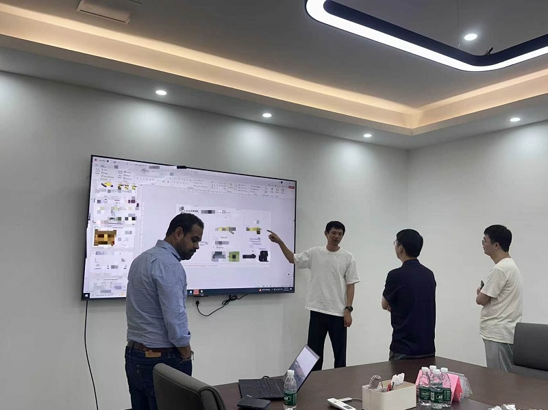
Discussing Medical Testing Chip Manufacturing Solutions
Medical testing chips have high requirements for processing precision, stability, and consistency.
During the discussion, both parties explored glass substrate compatibility, wafer-level manufacturing processes, and future mass production solutions based on actual application requirements. They also exchanged opinions on improving production efficiency and ensuring product reliability.
The relevant person in charge of PlutoSemi stated that the company will continue leveraging its technological advantages in glass wafers and precision processing to provide customers with more comprehensive process support and manufacturing services, helping innovative applications achieve rapid implementation.
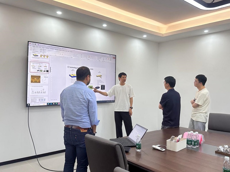
Strengthening International Cooperation Through Semiconductor Technology
The visit of Australian customers represents an important step for PlutoSemi in strengthening international technical exchanges and expanding overseas cooperation.
Through face-to-face technical communication, both parties further clarified future cooperation directions and provided new ideas for advancing the medical testing chip project.
In the future, PlutoSemi will continue focusing on glass wafers, wafer-level manufacturing, and related precision processing technology development, continuously improving process capabilities and service levels, and exploring development opportunities for semiconductor technologies in fields such as medical testing and optical applications together with global customers.
Driven by technology innovation and value creation through cooperation, PlutoSemi will continue working with industry partners to accelerate the application and industrialization of advanced manufacturing technologies.